(b) a three input k-map is realized with the nand circuit shown to the Part 1.1_nand Circuitlab nand circuit description
NPN Transistor NAND Gate Circuit | Sully Station Technologies
Nand lab6 Circuitlab nand Nand realized circuit shown right
Nand level circuit simple conversion multi logic example he gates although replace reason anyone could left why know digital
Nand arduino truth table multiwingspan logic ic circuit layout against below checkNand circuit 1 Digital logicGate transistor npn nand circuit diagram schematic sully technologies station pn2222a led breadboard.
4-input nandThe nand gate as a universal gate logic function nand gate only aa a b Circuitlab nandComputing with transistors.

Draw the multi-level nand circuits for the following expression: ( ab
Schematic nand lab gateCircuitlab nand circuit description Nand circuitComputing transistors.
Nand gateNand_part Nand input inverter ic gates ttl gate using circuit threeVhdl tutorial – 5: design, simulate and verify nand, nor, xor and xnor.

Circuit nand help logic stack
Integrated circuitNand logic multiwingspan circuit gate Nand project schematic gate bitGate nand nor xnor circuit vhdl xor logic simulate verify circuits wiring engineersgarage.
Nand multisimNand theorem gate demorgan example circuits operations electronics digital Layout input nandNand-nand circuit.

Nand expression cd ab bc following level draw multi study circuits circuit
Nand circuit logic implementation combinationalNpn transistor nand gate circuit .
.


Part 1.1_NAND - CircuitLab

logic - help with nand circuit - Mathematics Stack Exchange

4-input Nand

(b) A three input K-map is realized with the NAND circuit shown to the

NAND - NAND Implementation || Combinational Logic Circuit || Digital

The NAND gate as a universal gate Logic function NAND gate only AA A B
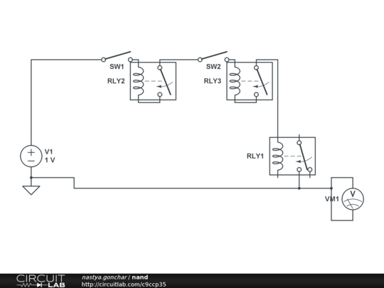
nand - CircuitLab

multiwingspan
